Roadmap to quantum dot qubit arrays using FDSOI
Researchers from France have highlighted a roadmap to building qubits for quantum computers using today’s FDSOI silicon on insulator process technology.
Silicon spin qubits represent one of the most promising avenues to achieving practical quantum computing, and new research into room-temperature parametric test procedures supports both their strong performance potential and the opportunities to ease their transition into manufacturing by using well-characterized processes and materials from the semiconductor sector.
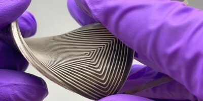
In an invited paper at the 2022 IEEE VLSI Symposium on Technology & Circuits, researchers from CEA-Leti, Université Grenoble Alpes, CNRS Institut Néel, and CEA-Irig shared a new three-step characterization chain for linear silicon quantum dot (QD) arrays fabricated on fully depleted silicon-on-insulator (FDSOI) material.
The team also offered several proposals for methodologies and metrics that can accelerate learning cycles at 300K, while generating statistical data on expected device performance at cryogenic temperatures.
Related quantum dot articles
- Quantum dot boost for quantum computing
- European startup ships first commercial quantum processor
- European project for commercial silicon quantum processor
- CEA-Leti to build silicon photonic quantum computer
The three-step approach maximizes the effectiveness of higher-temperature testing as part of the broader push towards making silicon QD devices manufacturable, by enabling developers to detect and analyze issues at the earliest and simplest point. “It’s a powerful step towards industrialization,” said Dr. Maud Vinet, quantum computing program director at CEA-Leti.
The initial wafer-level room temperature characterization step, which uses transistor-like testing protocols to gather data in a matter of hours, is followed by a more time-consuming wafer-level QD characterization step at less than 2 degrees K, and a die-level qubit manipulation step (which can take days per device) at under 100mK.
该研究小组使用过程评估切断al considerations related to production of integrated QD arrays and make recommendations for addressing them.
One such consideration relates to the proposed use of linear arrays of floating-gate QDs to operate in a manner similar to a single-gate standard transistor. The researchers found that inner gates in these arrays offer consistent state-of-the-art performance on threshold voltage (Vth) and subthreshold slope (SS), but outer gates exhibit more variability. The researchers propose dealing with these edge effect peculiarities (which can be caused by factors like random dopant fluctuation) by using the outer gates as access gates rather than for confinement of QDs.
While the split-gate design being explored for linear QD arrays offers several functional advantages, its successful implementation will require very strict overlay control on one specific lithography step to achieve good symmetry, which is needed for consistent performance.
A third recommendation is focused on the issue of spurious dots within the qubit layer — a major source of yield loss in silicon QD arrays. Spurious dots can be detected during cryogenic testing, but revealing the inter-gate defectivity that causes them earlier in the characterization chain (such as during 300K tests) would greatly accelerate the learning cycle.
Although standard transistor parametric tests are unsuitable for the task, the researchers developed a 300K voltage-sweep technique capable of monitoring the screening effect inter-gate defectivity has on exchange gate polarization.
Other quantum computing articles
- D-Wave steps up battle for quantum computers
- First room-temperature quantum computer in supercomputing centre
- EU Foresight report highlights semiconductors, quantum and space
- Sweden to build its own quantum computer
- Open design for large scale quantum computer
一个关键的力量FDSOI材料中使用group’s efforts, said Vinet, is the fact that back gates can be used to draw charges away from the interfaces. Back gates are typically fabricated using dopant implantation, which has the potential to introduce defects or parasitic dopants in the qubit layer. An alternative fabrication approach, using a TSV-like metallic back gate electrode, would be a way to alleviate this drawback while also enabling back-biasing, she added.
“These research results represent a significant step towards addressing the broader silicon spin qubit integration challenges we discussed at last December’s IEDM conference,” said Heimanu Niebojewski, CEA-Leti lead device engineer. “It’s a very encouraging sign of the technology’s maturation.”