€1.4亿欧元3D芯片研究中心在德累斯顿开业

Fraunhofer IPMS and Fraunhofer IZM-ASSID have opened a flagship €140m research centre for 3D chips in Dresden, Germany.
The Centre for Advanced CMOS & Heterointegration Saxony will provide the complete value chain for 300 mm wafer technology to build 3D chips and heterogeneous systems using substrates and chiplets. It will also work on ways to build neuromorphic and photonic AI and quantum devices on 300mm CMOS wafers.
The two organisation are the only two German research centres for applied microelectronics research based on 300 mm wafer industry standard equipment, working with semiconductor companies and system users as well as material and equipment manufacturers worldwide.
The centre also aims to tap into funding for the European CHIPS Act which aims to boost semiconductor production across the continent. Dresden is the centre of semiconductor production for Europe, although Intel chose another region in Germany, Madegeburg, for its leading edge fab backed by CHIPS Act funds.
Related articles
Fraunhofer IPMS将在洁净室设施和300mm前端晶圆处理设备上投资约1.4亿欧元,而Fraunhofer IZM-assID正在提供包装和系统集成技术。
该中心将由CNT的部门经理兼Fraunhofer IPMS副局长Wenke Weinreich博士和IZM-Assid网站经理ManuelaJunghähnel博士领导。
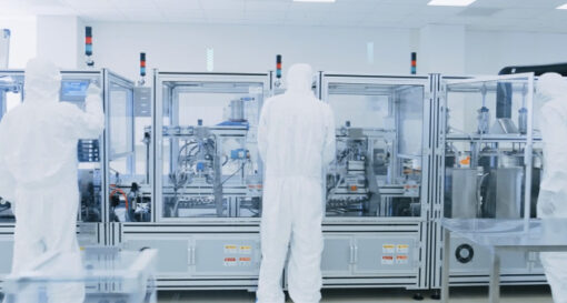
The Centre Nanoelectronic Technologies (CNT) is a business unit of IPMS and has 4000 m² of clean room space of class 6 and 3 (according to ISO 14644-1) as well as laboratory space for more than 80 processing and analytical tools are available. The equipment pool includes deposition and etching equipment as well as inspection and analysis equipment for determining defects and measuring layer properties.
IZM-ass具有基于铜直播的3D晶片级系统集成的200-300毫米技术系列。Fraunhofer izm-assID的过程线是专门为ISO 9001的面向生产和行业兼容的开发和处理而设计的。该系的组件是用于TSV形成的过程模块,用于TSV后TSV处理,用于TSV后处理(稀疏和分离)(稀疏和分离))和3D堆栈形成。
“The joint centre with a clean room of 4000 m² in size enables close cooperation and networking of the scientific and technical competencies of both research institutions. This creates an outstanding R&D technology platform as well as an increase in efficiency and completion of the value chain, which at the same time opens up new research fields,” said Dr. Manuela Junghähnel.
“ 300毫米晶圆的行业标准至关重要,因为这是确保将研究结果快速转移到萨克森州,全国和全球的半导体行业的唯一方法。另一方面,这种晶圆标准也是对未来技术(例如神经形态和量子计算)高科技研究的基本要求。” Wenke Weinreich博士说。
“每三个欧洲芯片都是在萨克森州自由状态生产的。通过《欧洲筹码法》,欧盟为进一步的投资设定了课程。新的Fraunhofer半导体研究中心在德国是独一无二的,将对硅萨克森州的创新做出决定性的贡献。将来,与最先进的300mm晶圆的应用微电子研究将在德累斯顿进行世界一级。
The R&D will be designed and expanded in such a way that local and national industry from SMEs to large companies such as Globalfoundries, Infineon and Bosch will be able to benefit from the latest technologies. The integration platform is also used in customer-specific projects as part of the High-Performance Research Fab Microelectronics Germany (FMD).