三星在3NM节点中引入纳米片晶体管
技术新闻
|
三星电子宣布了每年的流程节点路线图的更新,并引入了3NM登机口(GAA),据报道将在2022年或之后到达一段时间。在2017年。阅读更多
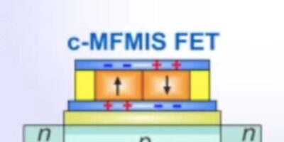
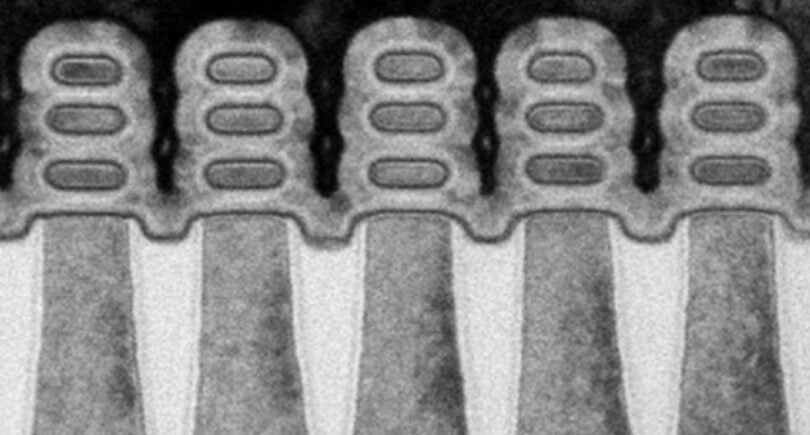
3海里有两种变体- 3 gaae和过程3GAAP – standing for early and plus and will be based on the nanosheet construction with multiple lateral ribbon-shaped wires in a fin. This nanosheet design has been much discussed by research institute IMEC as a follow-on to the FinFET and was researched by IBM in collaboration with Samsung and Globalfoundries.
“将GAA结构应用于我们的下一代流程节点将使我们能够领导开放一个新的智能,连接的世界,同时也可以增强我们的技术领导力。”三星电子。
此外,三星表示,其7nm 7LPP的过程正在为2018年下半年准备生产。三星将在2018年开始生产其自己的Exynos处理器为智能手机的处理器,但是通过三星铸造厂为Fabless Chip Companies提供的可用性可能必须等到2019年。这也可能是三星将在2018年不使用Extremulastaviolet Sivelography(Euvl)引入该过程(euvl(euvl))并在2019年插入euvl
但是,2017年同等事件的6nm流程已经从路线图中消失了(请参阅三星将4NM和FDSOI流程添加到路线图)。
三星宣布:
7LPP(7nm低功率加):7LPP是使用EUV光刻解决方案的第一个半导体工艺技术,该技术在2018年首次生产正轨。
+更多的