萨姆松上启用3 nm设计工具g process
The 3nm design flow and process are described as being suitable for applications in automotive, mobile, data center and artificial intelligence (AI).
The certification means that mutual customers of Cadence and Samsung Foundry have immediate access to circuit design, layout, signoff and verification tools and can begin their 3nm IC designs.
The custom and analog mixed signal (AMS) flow includes the Virtuoso ADE Suite, Virtuoso Schematic Editor, Virtuoso Layout Suite, Virtuoso Layout Suite Electrically Aware Design (EAD), Spectre X Simulator, Voltus-Fi Custom Power Integrity Solution, Quantus Extraction Solution, Litho Physical Analyzer (LPA), LDE Electrical Analyzer (LEA), Innovus Implementation System, and Pegasus Verification System.
“We have validated the Cadence AMS tools along with the entire flow, and it meets our requirements for designing with 3nm GAA process technology,” said Sangyun Kim, vice president responsible for the foundry design technology team at Samsung Electronics, in a statement issued by Cadence. He added that the design flow is available immediately.
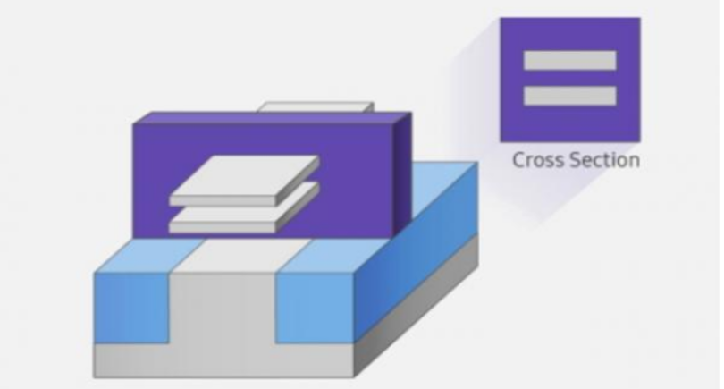
Samsung began volume production of 7nm FinFET designs at its ‘V1’ extreme ultraviolet lithography manufacturing line Hwaseong, South Korea, late in 2019. That 7LPP process has a successor, 5LPE, that has been defined for IP re-usability, yield learning leverage, and easy migration from 7LPP.
+MORE