imec shows backside power delivery with buried power rails

比利时研究实验室IMEC正在使用纳米直线递送的逻辑芯片进行逻辑芯片的第一次实验证明,该方案使用纳米直线递送(NTSVS)降落在埋藏的功率导轨(BPRS)上。
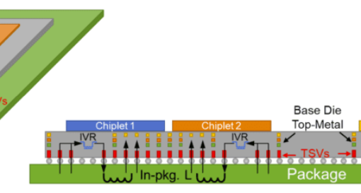
This is a key technology for future 2.5D and 3D chips built on 2nm process technology and shown at the 2022 IEEE VLSI Symposium on Technology and Circuits in the US this week.
BPRS连接到缩放的FinFET设备,其性能不受背面晶圆处理的影响。这也通过在晶圆的背面增加电容器来提高功率传递和性能提升,从而提供了系统性能优势。
臀部力量delivery allows to decouple the power delivery network from the signaling metallization scheme in logic chips, reducing the routing congestion. Since imec’s first announcement in 2019, different implementations have been proposed. At VLSI 2021 imec for the first time showed backside connectivity through nTSVs landing on metal-1 pads in the wafer’s frontside.
Related articles
- 臀部力量opens up new realms in chip design
- 臀部力量is key to Intel process
- imec, ARM demonstrate backside power delivery
- Delivering power from the back of a chip
- Applied upgrade supports backside power and GAA transistors
“We believe that combining backside power delivery with buried power rails – a structural scaling booster in the form of a local power rail that is buried deep in the chip’s front-end-of-line – is the most promising implementation scheme of a backside power delivery network in terms of scalability and performance,” said Naoto Horiguchi, Director CMOS Device Technology at imec.
“With our test vehicle, in which nTSVs land on buried power rails defined in the wafer’s frontside, we show that the performance of the FinFETs is not degraded by backside processing,” he said. “This includes bonding of the wafer to a carrier wafer, wafer backside thinning and processing of ~320nm deep nTSVs. The nTSVs land on BPRs with tight overlay control and are implemented at a tight pitch of 200nm without consuming any area of the standard cell. This ensures further scalability of the technology towards 2nm and beyond.”
“In a 2022 VLSI paper by R. Chen et al., we combined backside processing with the implementation of a 2.5D (i.e., pillar-like) metal-insulator-metal capacitor (MIMCAP), which serves as a decoupling capacitor,” said Eric Beyne, VP R&D of imec’s 3D System Integration. “The 2.5D MIMCAP boosts capacitance density with a factor of 4 to 5x, allowing a further improvement of the IR drop (32.1%/23.5% over the no-MIMCAP/2D-MIMCAP counterparts, respectively). The results are derived from an IR drop modelling framework calibrated with experimental data.”
“Our work shows that the backside can create a very dynamic design space with new design options that can help address shortcomings of traditional 2D IC scaling,” said Beyne. “In addition, we have shown its validity for 3D system scaling technologies, where the carrier wafer in de bonding process is replaced with a functional wafer with a logic wafer for enabling logic-on-logic 3D-SOCs, and the bottom dies are powered from the backside.”