

Developing on-board charging systems in electric vehicles: Challenges and solutions
v\:* {behavior:url(#default#VML);}
o\:* {behavior:url(#default#VML);}
w\:* {behavior:url(#default#VML);}
.shape {behavior:url(#default#VML);}
Normal
0
false
false
false
false
en - us
X-NONE
AR-SA
/* Style Definitions */
table.MsoNormalTable
{mso-style-name:”Table Normal”;
mso-tstyle-rowband-size:0;
mso-tstyle-colband-size:0;
mso-style-noshow:是的;
mso-style-priority:99;
mso-style-parent:””;
mso-padding-alt:0cm 5.4pt 0cm 5.4pt;
mso-para-margin-top:0cm;
mso-para-margin-right:0cm;
mso-para-margin-bottom:8.0pt;
mso-para-margin-left:0cm;
line-height:107%;
mso-pagination:widow-orphan;
font-size:11.0pt;
font-family:”Verdana”,sans-serif;
mso-ascii-font-family:Verdana;
mso-ascii-theme-font:minor-latin;
mso-hansi-font-family:Verdana;
mso-hansi-theme-font:minor-latin;
mso-ansi-language:EN-US;
mso-fareast-language:EN-US;}
By
丹尼尔Makus, Application Marketing Manager, Charging infrastructure and Applications in Electrified Powertrain, and
Lisa Holzmann, Application Engineer, Discrete semiconductors for On-board chargers and DC-DC converters, both atInfineon Technologies
介绍
The on-board charging system built into electric vehicles (EV) and plug-in hybrid vehicles (PHEV) is a central element. Responsible for converting AC voltage from the power grid into DC charging voltage for the battery, theon-board chargermust meet the requirements of the grid on the infrastructure side and those of the manufacturer on the vehicle side.
The on-board charger consists of a power factor correction stage (PFC) and a galvanically isolated DC/DC converter, primary and secondary side (Figure 1).
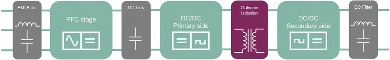
Figure 1.Block diagram of an on-board charger for electric vehicles and plug-in hybrids.
650 VSi superjunction MOSFETsand 750 Vsilicon carbide (SiC)MOSFETs are the right choice for 400 V batteries. In the case of 800 V batteries used in the premium segment, however, SiC power semiconductors with breakdown voltages of 1200 V are preferred.
Selecting the right PFC stage topology
Most PFC circuits are operated in continuous current mode (CCM). This requires semiconductors such as Infineon’sCoolSiCTMMOSFETsor fast switchingIGBTsin combination withCoolSiC™ diodesthat are resistant to hard commutation on their body diode.
The simplest topology for a PFC is the boost converter, enabling single-phase unidirectional power flow from the AC input to the DC output.
With a similar operation, the interleaved boost topology consisting of two boost converters offers a more flat efficiency. However, the overall efficiency is still limited by the diode bridge rectifier.
A more efficient topology is the totem-pole PFC circuit, which is also suitable for bidirectional operation. Here, all diodes are replaced by active power switches, allowing a power flow in both directions.
Efficient DC-DC converter stage topologies
DC-DC converters often consist of a ZVS phase-shift full bridge or an LLC topology. The benefits of the phase-shifted full bridge are its high efficiency since it can be operated in soft switching over a wide load range with the exception of very low loads. It achieves a higher conversion ratio compared to an LLC converter. Moreover, if the secondary side is actively switched and a suitable control strategy is used, the phase-shifted full bridge is also suitable for bidirectional operation, becoming a Dual Active Bridge topology.
On the other hand, LLC converters offer better peak efficiency and, therefore, higher power density. Zero voltage switching is possible over the entire load range. However, hard-switching still occurs during start-up and under some critical conditions, which is why MOSFETs with a fast body diode should be used with this topology. If the LLC converter is modified by additional passive components on the secondary side so that the resonance circuit is balanced, a bidirectional operation is feasible, for example, in the form of a CLLC topology.
Cooling and packaging for higher power density
For high power density, the cooling of the power components and their package plays an important role. The best solution for this is top-side cooling, as supported by Infineon, for example, in the form of theQDPAK package(Figure 2). By using top-side cooling, the power density is increased as both sides of the PCB sides can be assembled. In addition, the power circuits can be optimized, and heat is decoupled from the PCB, which allows higher junction temperatures.

Figure 2.Infineon’s QDPAK package allows power semiconductors to be cooled through the top of the package.
One option of assembly is to insert a thermally conductive gap filler between the components and the heat sink to compensate for the different component heights, as well as a thermal insulation material to meet the OEM isolation voltage requirements (Figure 3).

Figure 3.Insertion of a thermally conductive gap filler to compensate for the different component heights.
For more information on Infineon’s broad portfolio of products and solutions for on-board battery chargers, please visit our related网页.

