Samsung embeds AI accelerator in memory chip
window.dataLayer = window.dataLayer || [];
function gtag(){dataLayer.push(arguments);}
gtag(‘js’, new Date()); gtag(‘config’, ‘UA-160857065-1’);
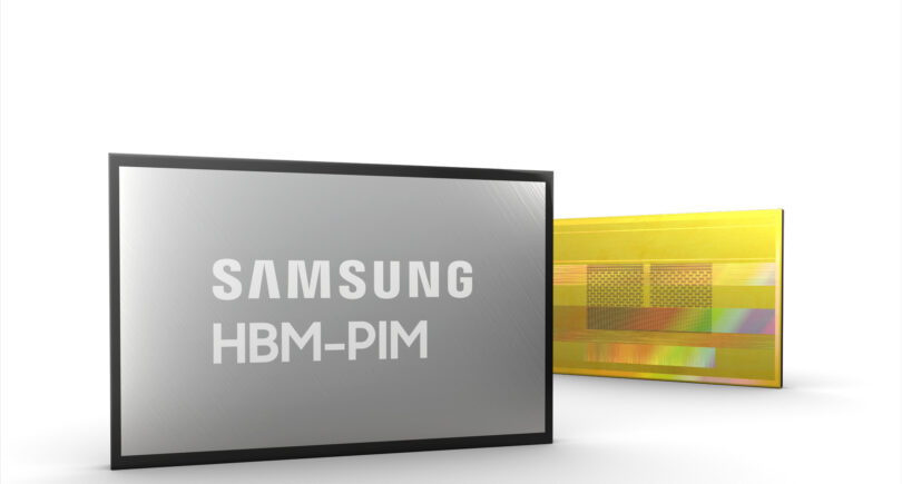
Samsung Electronics has added an AI accelerator into a high speed memory chip for in-processing memory. The 4Gbit HBM-PIM DRAM, shown at the ISSCC conference this week, is the industry’s first High Bandwidth Memory (HBM) integrated with AI for processing-in-memory (PIM).
The combined architecture brings AI computing inside high-performance memory for large-scale processing in data centres and high performance computing (HPC) systems but Samsung is also looking at using the technology in AI-enabled mobile applications.
“Our HBM-PIM is the industry’s first programmable PIM solution tailored for diverse AI-driven workloads such as HPC, training and inference. We plan to build upon this breakthrough by further collaborating with AI solution providers for even more advanced PIM-powered applications,” said Kwangil Park, senior vice president of Memory Product Planning at Samsung Electronics.
The HBM-PIM brings processing power directly to where the data is stored by placing a 300MHz, 16bit floating point AI engine, which Samsung calls a Programmable Computing Unit (PCU) inside each memory bank to minimise data movement. This means there are 32 of the FP16 PCUs for a 4Gbit DRAM die to handle the weights in an inference engine.
Used with Samsung’s existing HBM2 Aquabolt memory interface, the new architecture is able to deliver over twice the system performance while reducing energy consumption by more than 70 percent. The HBM-PIM also does not require any hardware or software changes, allowing faster integration into existing systems, and Samsung has stacked four of the HBM-PIM 4Gbit die with four standard 8Gbit die for use in AI accelerators.
Next: Testing out the HBM-PIM chip
The HBM-PIM chip is now being tested inside a range of datacentre AI accelerators, expected to be Nvidia and AMD who both support HBM2 interfaces, with all validations expected to be completed within the first half of this year. One of the first users of the chip is in the supercomputer used by the Argonne lab in the US.
“我高兴地看到,三星是解决the memory bandwidth/power challenges for HPC and AI computing. HBM-PIM design has demonstrated impressive performance and power gains on important classes of AI applications, so we look forward to working together to evaluate its performance on additional problems of interest to Argonne National Laboratory,” said Rick Stevens, Argonne’s Associate Laboratory Director for Computing, Environment and Life Sciences.